Laboratory
Dalectro is specialised in analysis and test of printed circuit boards.
With our metallographic sampling equipment and microscopes we are also able to analyse assemblied boards, single electronic components, solderjoints, encapsulations, contacts, pressfit, crimping, surface treated finemechanics, sheet metal and similar.
X-ray or microsection?
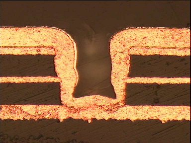
X-ray is an excellent and fast method for finding defects in pcb innerlayers, voids and cracks in solder joints and components. But the X-ray resolution is limited and without colors. Microsections (cross sections) add the extra details and colours. Metallographic samples visualise details down to 0,5 µm and reveals different metal layers, conjunctions and intermetallics (IMC), which no other test method can offer.
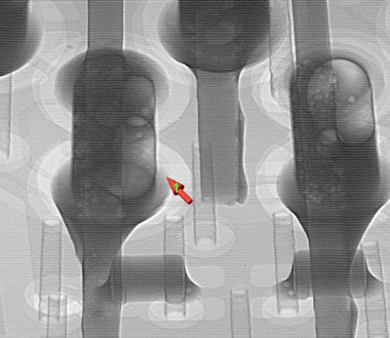 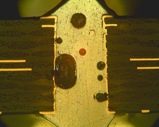
3D X-ray of a solder joint with voids Microsection of the same solder joint
Our test equipment
We have equipment for visual control, thermal chock and microsection analysis (cross- section) in our own independent laboratory.
- Metallurgic optical microscope
- Stereozoom optical microscope
- Digital microscope camera with measurement software
- Digital high resolution camera
- Diamond blade wet cutting equipment
- Metal bandsaw wet/dry for large details
- Bandsaw dry for large non-metallic details
- Beltsanders for non-metallic details
- Grinding- and polishing equipment for microsection preparation
- Ultrasonic cleaning equipment - low effect
- Solderpot for leadfree thermal tests and solderability tests
- Solderpot with lead for thermal tests and solderability tests
- Sandfilled pot for thermal chock without solder
We can also perform measurements with external partners:
- Measurement with XRF of nm thin layers like gold, nickel, silver
- Control of bondable surfaces (ball bonding and wire bonding)
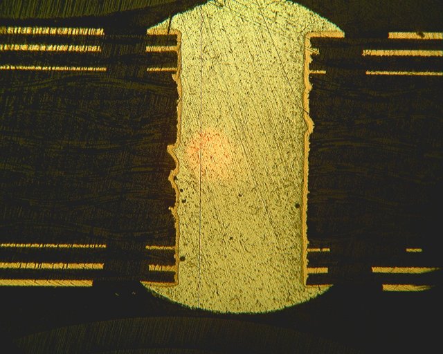
Microsections
The printed circuit board integrity and the different internal properties can be detail analysed only by microsections (cross-sections). Microsectioning reveal all kind of internal defects and can also show process indicators for material and processes, but also give at hand if design or material selection might be incorrect.
Dalectro can perform simple and rather quick microsection sampling, to more thorough fault analysis with extensive sample preparation, picture material and measurements.
Sampling and analysis under microscope can be done at several levels, depending on defect type, root cause and required sampling extent and required final finish on the samples.
 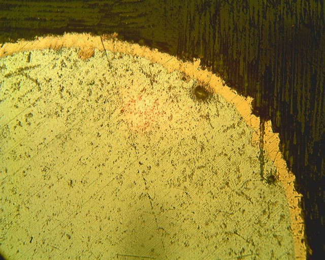 
Vertical conventional microsection Horisontal microsection is Microvia - Etched sample in order
is the most common sample method time consuming but revealing to reveal metal layer boundaries
Microsections are destructive and can be conducted at both assemblied boards and bare printed circuit boards.
What we can measure
The metallurgical microscope makes it possible to visualise and measure:
- Copper thickness in holes
- Copper thickness on inner and outer layer
- Base copper and plated copper thickness
- HASL and other plated metals (>0,5 µm) example Ni, Au, Sn, Ag
- Dielectric layers and soldermask
- Build-up, core and prepreg
- Hole diameter
- Board thickness
- Intermetallic layers
- Voids, cracks and delamination
- Tear out, back etch, wicking
For further information, please contact Esbjorn Johansson at Dalectro
Call +46 70 795 88 72 or email: esbjorn@dalectro.se
|
|