Image gallery
Laboratory
Our laboratory is equipped with metallographic microscopes and sample preparation machines and equipment for baking, thermal chock and solderability tests.
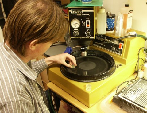 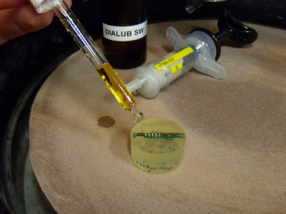 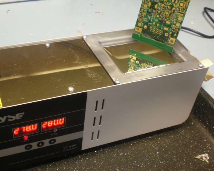
Microsection sample preparation Diamond polishing of pcba microsection Temperature chock of bare pcb
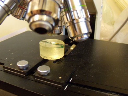 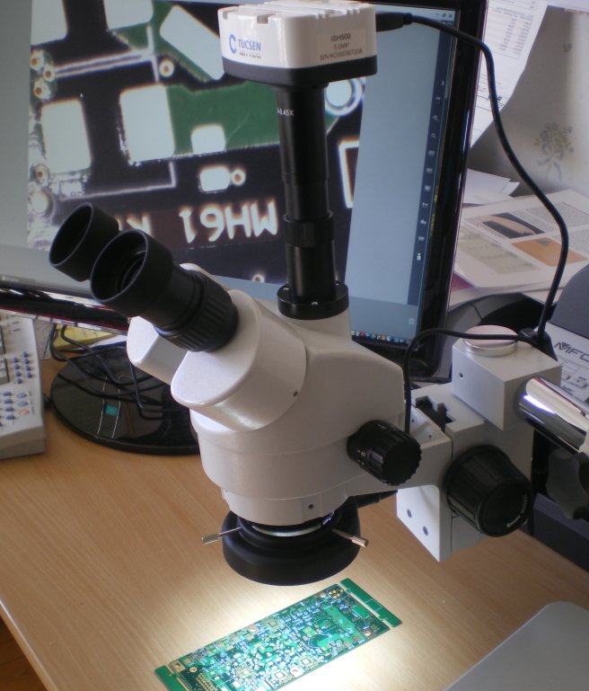 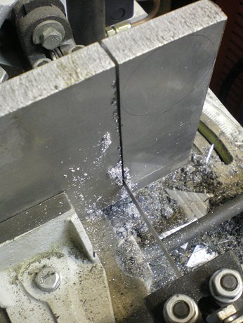
Microsection in metallurgic microscope Stereo microscope inspection of pcb Slow dry cutting of thick alumina plate
Defect examples
There are numerous variations of the most common defects and thousands of possible root causes, due to the vast number of manufacturing processes required for printed circuit board manufacturing.
What first appear to be printed circuit defects only, can in some cases be problems located in solderjoints and components as well.
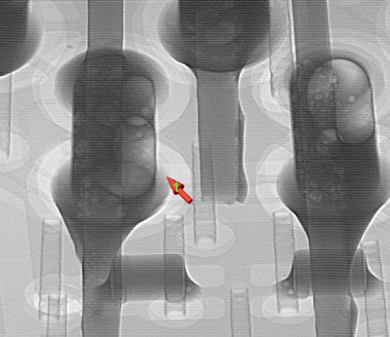  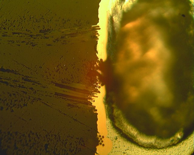
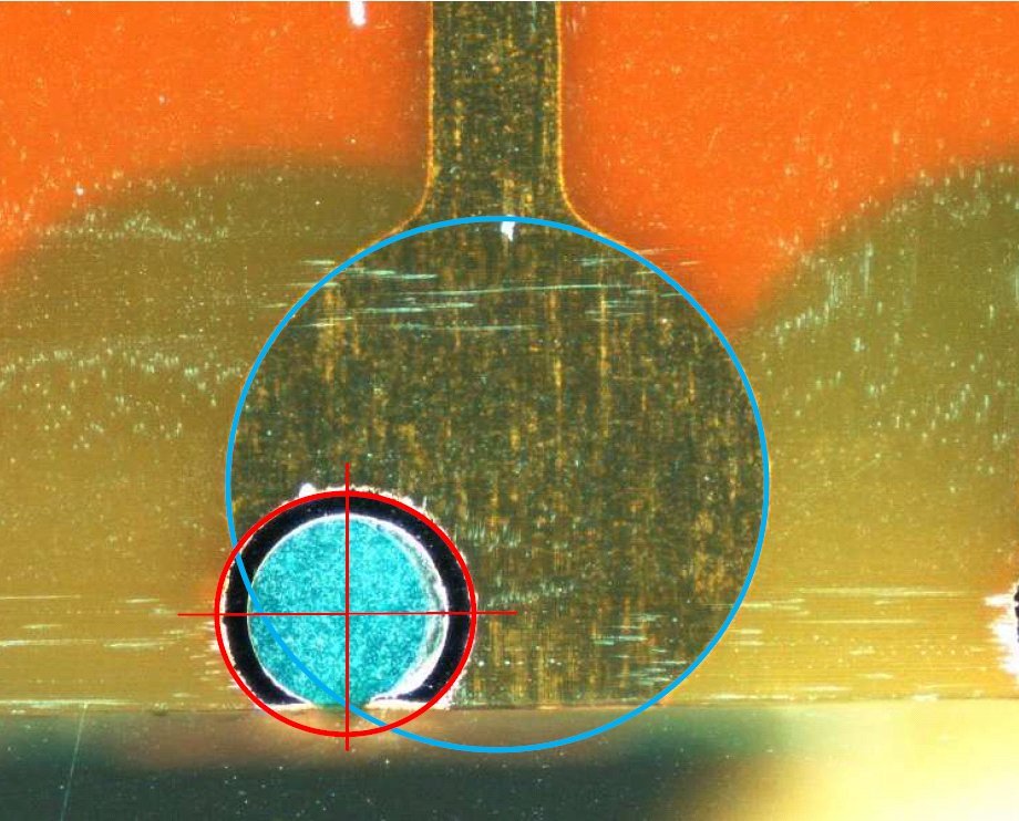
3D X-ray reveals voids in a solderjoint Microsection of the same solderjoint Plating void causing outgassing
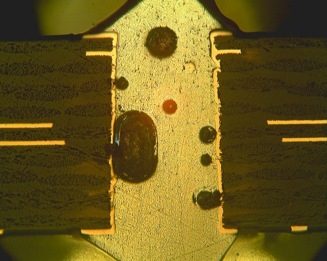
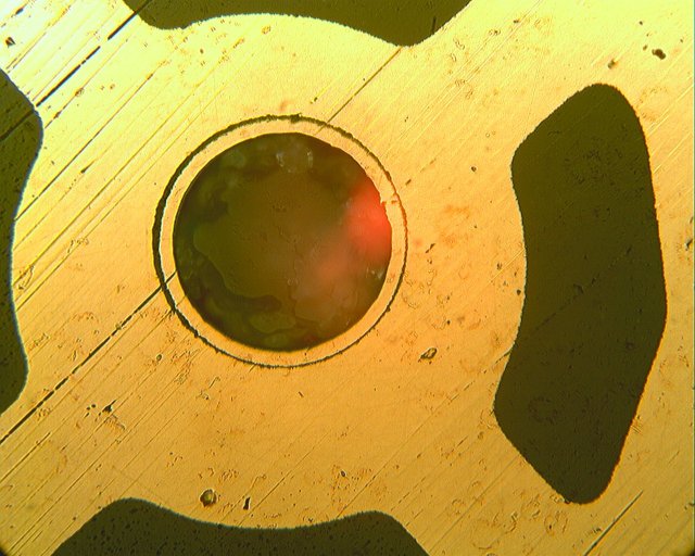
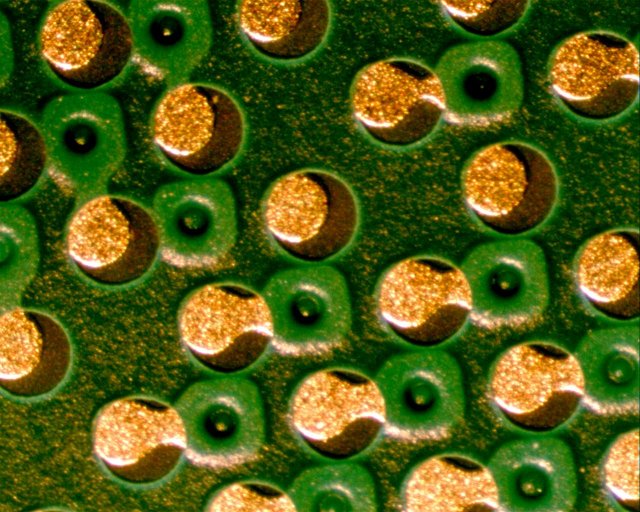
Stereoscope picture of resin filled and overplated blind vias Microsection of SMD capacitor solderjoint
 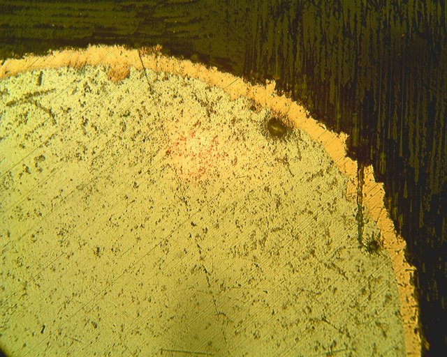 
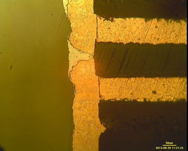
Vertical microsection is the most common Horisontal microsection Microvia with etched copper conjunctions
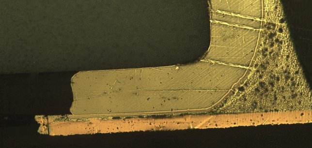
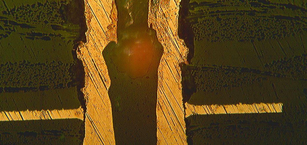
Horisontal microsection with break out Horisontal microsection shows smearing Thin HASL with exposed copper
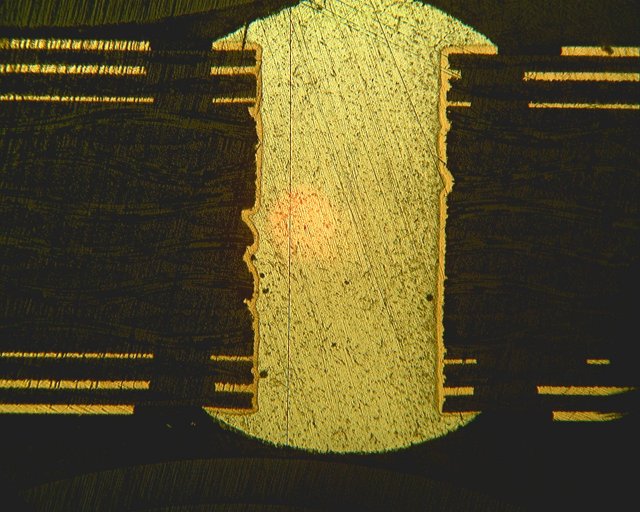
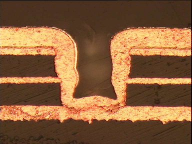
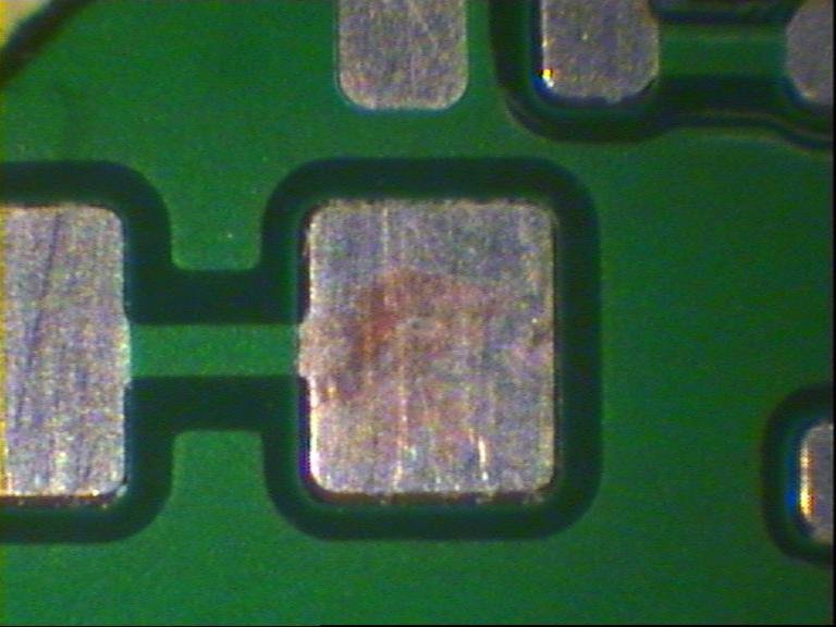
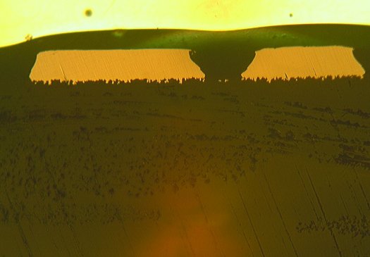
Innerlayer with resin smearing and breakout Plating thickness below IPC-requirement Soldermask misregistration around BGA pads
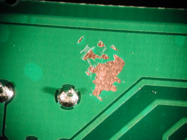  
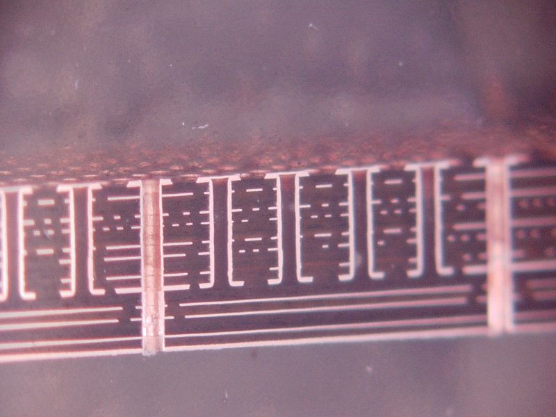
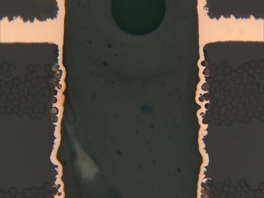
Soldermask peel off exposing copper Plating void centered at kapton flex layer Soldermask over impedance diff pair
|